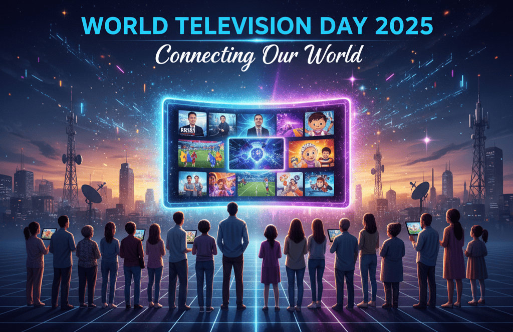
World Television Day – Celebrating a Medium That Changed the World Every year on November 21, the world honors a medium that brought nations closer, delivered unforgettable moments, and became
World Television Day – Celebrating a Medium That Changed the World Every year on November 21, the world honors a medium that brought nations closer, delivered unforgettable moments, and became
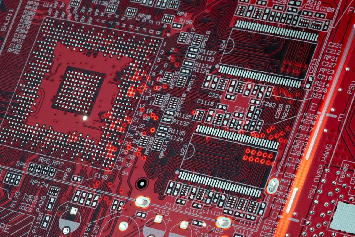
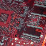
As the semiconductor industry races toward 2nm process technology, traditional EUV lithography faces physical limits in patterning ever-smaller transistors. High-NA EUV lithography emerges as the game-changing solution, offering higher resolution, improved yield, and the capability to power next-generation chips for AI, HPC, and mobile devices. This article explores the differences between EUV and High-NA EUV, the science behind advanced optics, the global adoption race led by ASML, Intel, TSMC, and Samsung, and why High-NA EUV is critical for shaping the future of chipmaking.
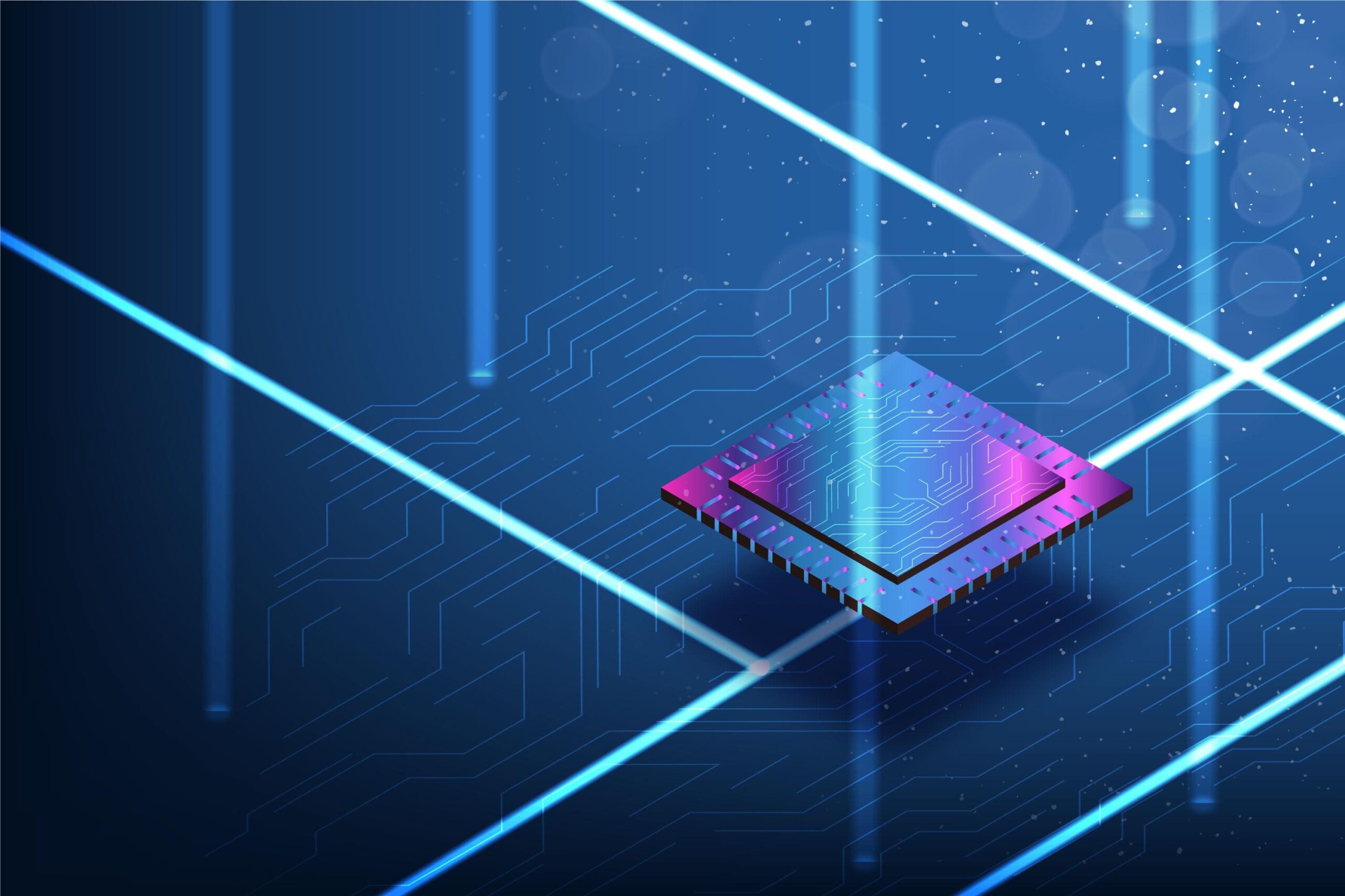
The semiconductor industry is entering a new era with High-NA EUV lithography, capable of printing features as small as 8 nm. Developed by ASML and adopted by Intel and SK hynix, it pushes Moore’s Law forward with 3× transistor density, higher yields, and lower complexity. From powering AI supercomputers to enabling next-gen memory and autonomous driving, the potential is enormous. While challenges like high costs and power demands remain, High-NA EUV is set to become the most transformative chipmaking technology of the decade.

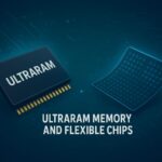
Discover how UltraRAM memory and flexible chips are revolutionizing the semiconductor industry. Explore their features, benefits, applications, and future impact on technology, IoT, and data storage.
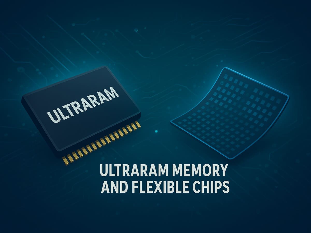
Discover how UltraRAM memory and flexible chips are revolutionizing the semiconductor industry. Explore their features, benefits, applications, and future impact on technology, IoT, and data storage.