In today’s digital economy, ai videos are no longer optional — they are essential. 🚀 Ready to Create AI Videos That Grab Attention?Stop struggling with complicated software. Let AI do
Explore the world of engineering, where innovation meets practical solutions. This category covers insights, trends, technologies, and real-world applications. Whether you’re a student, professional, or enthusiast, dive into articles that highlight the science, creativity, and impact behind engineering.
In today’s digital economy, ai videos are no longer optional — they are essential. 🚀 Ready to Create AI Videos That Grab Attention?Stop struggling with complicated software. Let AI do
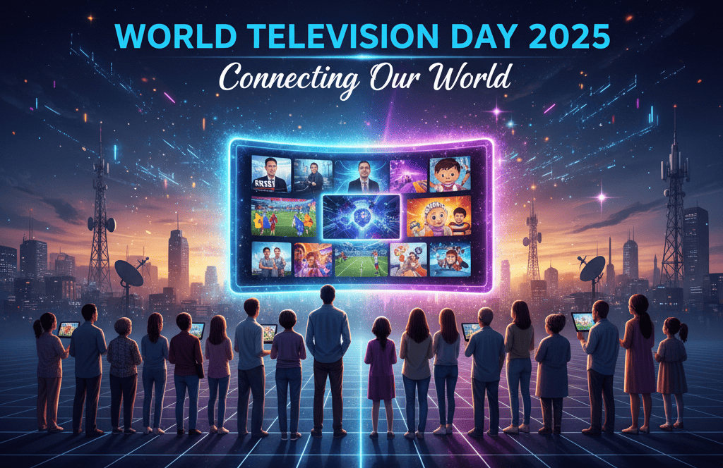
World Television Day – Celebrating a Medium That Changed the World Every year on November 21, the world honors a medium that brought nations closer, delivered unforgettable moments, and became

Updated: November 2025 | Author: Malhar Chauhan Introduction In 2025, every successful company runs on projects. The surge in project management skills 2025 demand proves how vital strategic leadership has become.
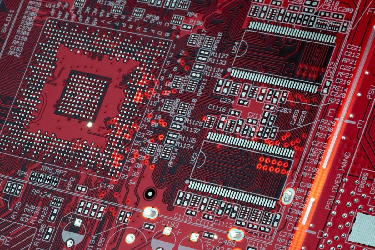
As the semiconductor industry races toward 2nm process technology, traditional EUV lithography faces physical limits in patterning ever-smaller transistors. High-NA EUV lithography emerges as the game-changing solution, offering higher resolution, improved yield, and the capability to power next-generation chips for AI, HPC, and mobile devices. This article explores the differences between EUV and High-NA EUV, the science behind advanced optics, the global adoption race led by ASML, Intel, TSMC, and Samsung, and why High-NA EUV is critical for shaping the future of chipmaking.

Discover how microwave and mmWave technologies enable IoT networks with high throughput, low latency, and scalability. Explore use cases in smart grids, factories, agriculture, healthcare, and smart cities, along with deployment best practices and future trends.

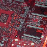
Flexible electronics are reshaping the future of technology—quite literally. From foldable smartphones and skin-like medical patches to lightweight solar panels and smart clothing, this new wave of bendable, stretchable, and wearable devices is transforming industries. In this blog, we explore how flexible electronics are moving from lab experiments to everyday life, highlight real-world success stories, and take a closer look at the startups leading the charge.
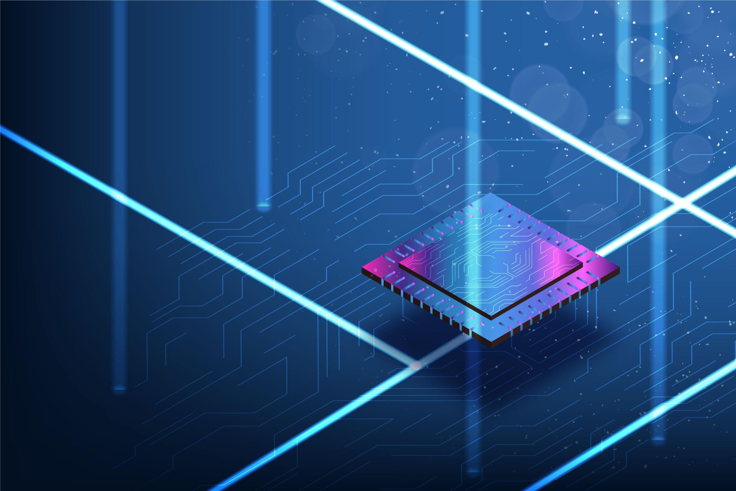
The semiconductor industry is entering a new era with High-NA EUV lithography, capable of printing features as small as 8 nm. Developed by ASML and adopted by Intel and SK hynix, it pushes Moore’s Law forward with 3× transistor density, higher yields, and lower complexity. From powering AI supercomputers to enabling next-gen memory and autonomous driving, the potential is enormous. While challenges like high costs and power demands remain, High-NA EUV is set to become the most transformative chipmaking technology of the decade.

Discover the 10 best AI tools to create professional videos in 2025. From text-to-video generators to realistic AI avatars, explore features, real-world use cases, and direct website links. Perfect for YouTubers, businesses, and creators looking to save time, cut costs, and produce engaging video content effortlessly.

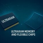
Discover how UltraRAM memory and flexible chips are revolutionizing the semiconductor industry. Explore their features, benefits, applications, and future impact on technology, IoT, and data storage.
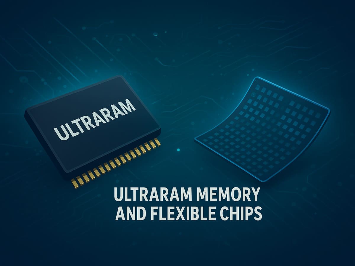
Discover how UltraRAM memory and flexible chips are revolutionizing the semiconductor industry. Explore their features, benefits, applications, and future impact on technology, IoT, and data storage.